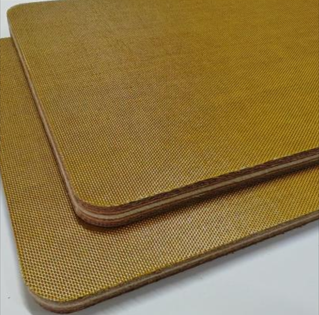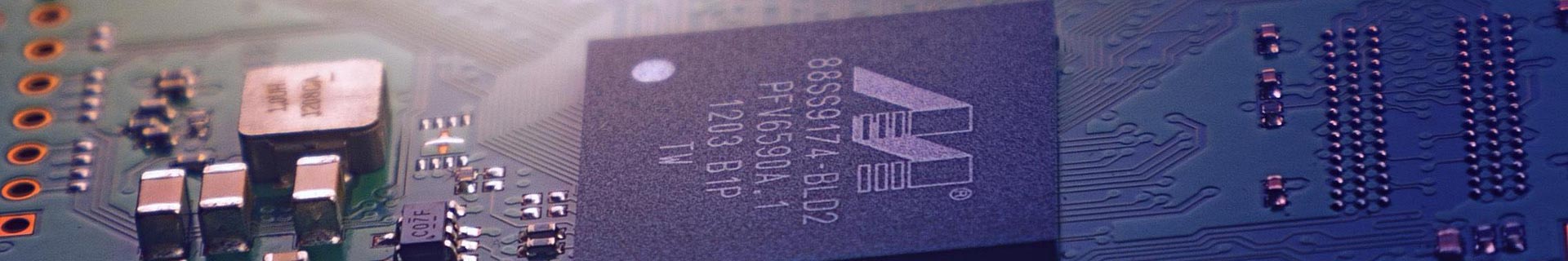
Fan-out Panel Level Packaging (FOPLP) represents one of the most significant convergences in the history of electronics manufacturing. By applying PCB-style large-format lamination to semiconductor packaging, the industry can achieve massive economies of scale.
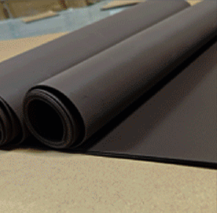
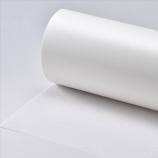
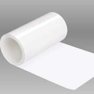
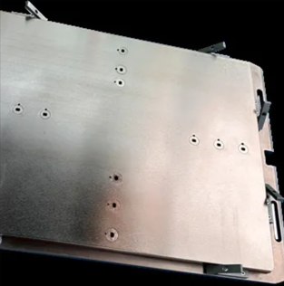
However, this "marriage" of technologies requires a significant upgrade in cleanroom-grade consumables. Traditional PCB tolerances are no longer sufficient; FOPLP demands micron-level flatness to ensure that fine-pitch interconnects are successfully bonded. This has led to the development of specialized semiconductor-grade carrier trays and zero-outgassing release films. These materials prevent any chemical contamination that could lead to device failure. As FOPLP gains traction in mobile and automotive chipsets, the quality of the lamination interface is becoming the new gold standard for advanced packaging.